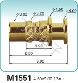
source:pogo pin release time:2021-09-23 Article author:sznbone Popular:POGO PIN
Theory and introduction of pogopin connector
The use of connectors simplifies the circuit board planning process. Smaller PCBs require equipment that cannot accommodate larger PCBs. Whether you squeeze a device or product onto one PCB or multiple PCBs, you need to consider power consumption, undesired signal coupling, the availability of smaller components, and the overall cost of the device or product, and so on.

In addition, the use of connectors simplifies the production and testing of electronic equipment. Simple and easy detection methods can greatly save costs. High-density circuit boards have more traces and components per unit area. A better method is to plan the equipment or product as multiple interconnected MDFs rather than a single high-density board, which depends on the investment in the complexity of the manufacturing plant.
Connector through-hole function allows the third dimension to connect traces and components on the PCB. In the horizontal and vertical direction, the top PCB can apply conductive copper traces along the PCB. Coupled with more layers of circuit boards, some single-layer PCBs will appear between the two sides of the double-sided PCB. A typical multilayer PCB has five layers with a thickness of less than 0.08 inches (2mm). It is a conductive internal surface that can transmit current between any two layers of a multilayer PCB.
Because of the complex technology, modern electronic equipment is more reliable and the cost is lower. PCB manufacturing of multi-layer boards has been a big challenge because of the hidden connections between two or more layers of copper traces. Surface mount technology (SMT) facilitates miniaturization, because components can be easily mounted on the PCB even without drilling holes. When using SMT, the robot device first pastes the adhesive component on the PCB, and then applies the adhesive to the underside of the component. The lead on the pre-tinned wire of the component and the lead on the pre-tinned pad on the PCB are reflowed or remelted. After the PCB is cooled, the soldering process is completed.
Pogopin connector introduction
1. Due to the long use time of the connector, a certain amount of dust or other small debris will accumulate inside. When dealing with these problems, please be careful not to use normal silk cloth wet with water to clean up, so as not to simply make the other inside the connector The component fails due to moisture.
2. Don't mess around with the metal chip on the pin side of the scraper board connector. Otherwise, once scratched, it will affect the working function and service life of the board. For example, it will cause some data transmission abnormalities in the potentiometer during use.
Three. Before using the pogopin connector, you should check whether the pogopin connector is incorrectly connected or fully locked, so as to avoid simple failures during use.
Read recommendations:
M3152 1.8x6.5(1A)Quick charging spring thimble factory
M3177 4.0X22.0(2A)E-cigarette pogo pin manufacturer
The development prospects of the core technology of the connector industry.
The impact of accuracy on the performance of the Pogo pin connector